
Semiconductor | Ultra-Pure Water Treatment Solutions
High-Purity Water for Semiconductor Manufacturing
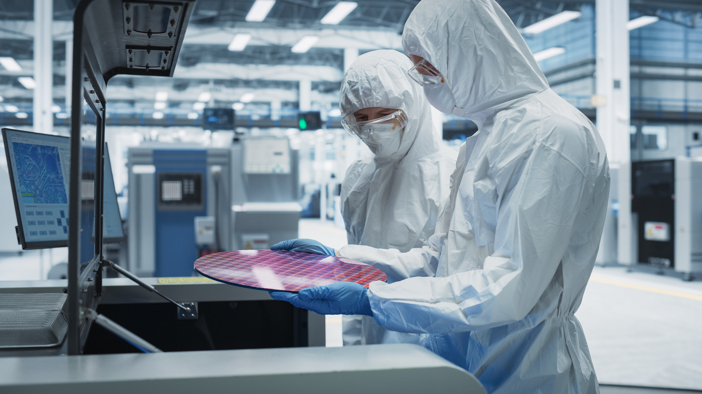
Water is an essential component in semiconductor fabrication, where ultra-pure water (UPW) is required for chip production, wafer cleaning, chemical dilution, and cooling systems. Even trace contaminants such as dissolved solids, organic matter, or bacteria can
lead to defects, reduced yield, and compromised semiconductor performance.
At Mueller Water, we specialize in cutting-edge water treatment solutions designed to meet the stringent purity requirements of the semiconductor industry. Our reverse osmosis, deionization, and advanced filtration systems ensure high-purity water production, optimizing process efficiency, yield rates, and regulatory compliance.
Importance of Ultra-Pure Water (UPW) in Semiconductor Manufacturing
Semiconductor fabrication requires extremely pure water for various stages of chip production, including:
- Wafer Cleaning & Etching – Removing particles, chemicals, and residues without introducing new contaminants.
- Chemical Dilution & Mixing – Ensuring process chemicals remain stable and effective.
- Steam & Cooling Systems – Preventing scaling, corrosion, and thermal inefficiencies.
- Rinsing & Final Processing – Achieving defect-free wafers for high-performance electronics.
Even contaminants as small as parts per trillion (ppt) can cause circuit malfunctions, reduced yield rates, and costly production losses.
Water Treatment Technologies for Semiconductor Applications
Mueller Water provides state-of-the-art water purification systems designed to produce ultra-pure water (UPW) meeting ASTM, SEMI, and ITRS standards:
1. Reverse Osmosis (RO) Filtration
- Removes 99% of dissolved solids, heavy metals, and organic compounds from feedwater.
- Essential for pre-treating water before further purification.
- Example: A semiconductor foundry in California implemented RO filtration, reducing total dissolved solids (TDS) from 500 ppm to <10 ppm, significantly improving wafer yield rates.
2. Deionization (DI) & Electrodeionization (EDI) Systems
- Produces ultra-pure, deionized water by removing ions, minerals, and silica.
- Used in wafer washing, chemical dilution, and final rinse applications.
- Example: A chip manufacturer in Texas installed an EDI system, achieving resistivity levels of 18.2 MΩ-cm, ensuring defect-free wafer production.
3. Ultraviolet (UV) Oxidation & TOC Reduction
- Eliminates organic contaminants and bacteria through UV light sterilization.
- Reduces Total Organic Carbon (TOC) levels to meet semiconductor-grade water standards.
- Example: A fab facility in Taiwan incorporated UV-TOC reduction, lowering TOC levels from 100 ppb to <5 ppb, preventing organic fouling on silicon wafers.
4. Nanofiltration & Ultrafiltration (UF)
- Removes colloidal particles, endotoxins, and microorganisms from process water.
- Protects RO membranes and extends system lifespan.
- Example: A semiconductor plant in South Korea installed ultrafiltration pre-treatment, reducing membrane fouling by 50% and improving UPW production consistency.
5. Advanced Wastewater Treatment & Reuse
- Enables semiconductor manufacturers to recycle and reuse process water, reducing water waste and costs.
- Chemical precipitation, RO concentrate recovery, and zero liquid discharge (ZLD) technologies help minimize environmental impact.
- Example: A fab facility in Arizona implemented a wastewater recycling system, cutting freshwater consumption by 40% and meeting strict environmental discharge regulations.
Benefits of Ultra-Pure Water Treatment in Semiconductor Manufacturing
1. Improved Wafer Yield & Process Reliability
- Prevents particle contamination, ensuring higher chip fabrication success rates.
- Supports consistent chemical formulations for precise wafer processing.
2. Reduced Equipment Downtime & Maintenance Costs
- Protects etching tools, chemical baths, and rinse stations from scaling and fouling.
- Minimizes shutdowns due to water quality issues, increasing production uptime.
3. Compliance with Semiconductor Industry Standards
- Meets SEMI F63, ASTM D5127, and ITRS water purity specifications.
- Ensures water resistivity of 18.2 MΩ-cm, TOC levels below 5 ppb, and minimal bacterial presence.
4. Environmental Sustainability & Cost Savings
- Wastewater treatment & recycling reduce water consumption and regulatory liabilities.
- Enhances corporate sustainability goals while lowering operational expenses.
The Risks of Untreated Water in Semiconductor Applications
Without proper water treatment, semiconductor fabs face serious risks that can impact production efficiency and product quality:
- Particle Contamination – Even sub-micron contaminants cause defects in integrated circuits (ICs), lowering chip yields.
- High TOC & Bacterial Growth – Organic matter in water reduces wafer cleanliness and can lead to process instability.
- Scaling & Corrosion in Equipment – Hard water minerals cause fouling in etching tools, cooling towers, and rinsing stations, leading to frequent maintenance and downtime.
- Regulatory Non-Compliance – Failure to meet semiconductor-grade water standards can result in product recalls, manufacturing inefficiencies, and financial losses.
Case Study: Ultra-Pure Water System for a Semiconductor Fab
The Problem:
A leading semiconductor foundry in Japan faced low wafer yield rates due to:
- High silica and TOC levels in process water, affecting photolithography precision.
- Frequent RO membrane fouling, increasing maintenance costs.
- Excessive wastewater discharge, impacting environmental compliance.
The Solution:
The facility partnered with Mueller Water to implement a multi-stage water purification system:
- Reverse Osmosis (RO) & Deionization (DI) for high-purity water production.
- Ultraviolet (UV) TOC Reduction to minimize organic contamination.
- Wastewater Recycling & Reuse System to reduce water waste.
The Results:
- Wafer yield rates increased by 12%, reducing chip defects.
- RO membrane lifespan extended by 40%, lowering maintenance costs.
- Total water consumption reduced by 35%, improving environmental compliance.
Contact Mueller Water for Semiconductor Water Solutions
Semiconductor manufacturing requires the highest level of water purity to ensure precision, efficiency, and regulatory compliance. At Mueller Water, we design and implement custom ultra-pure water treatment systems to support chip fabrication, wafer cleaning, and chemical processing.
Why Choose Mueller Water?
- Advanced water purification technologies for semiconductor-grade UPW.
- Customized solutions for process water, wastewater treatment, and recycling.
- Reliable support & maintenance for long-term efficiency.
Contact Mueller Water today to optimize your semiconductor water treatment system and improve production efficiency!
Recommended Mueller Products: